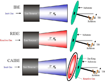
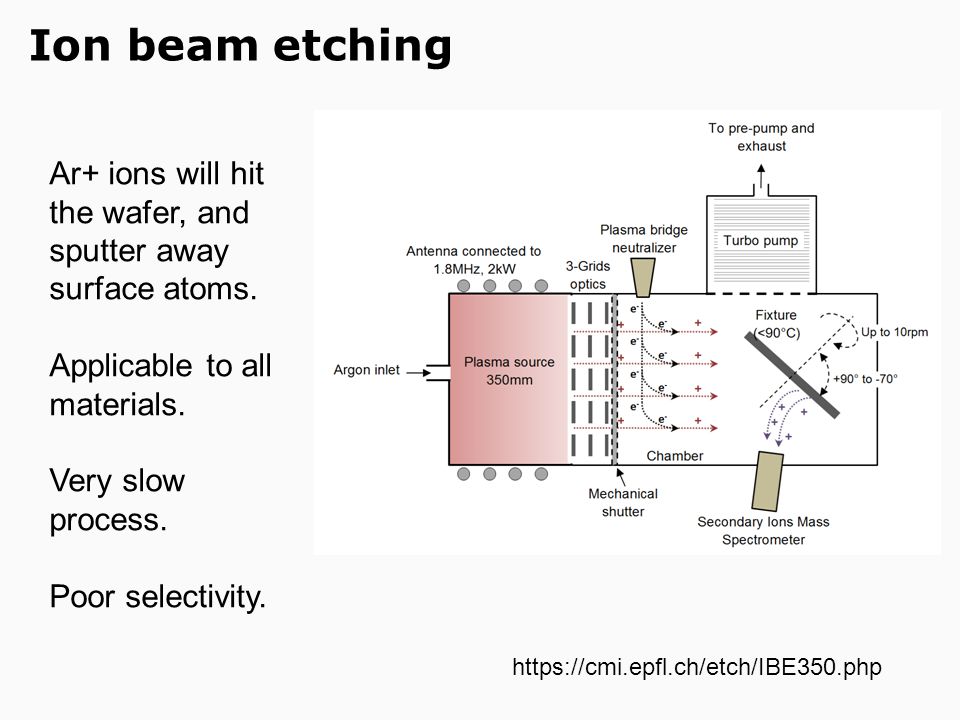
The ion beam etching ibe is a physical dry etch process.
Ion beam etching process.
The process is different from electric discharge electron beam laser and plasma arc machining in that the process does not depend on heating of the workpiece to the point of evaporation.
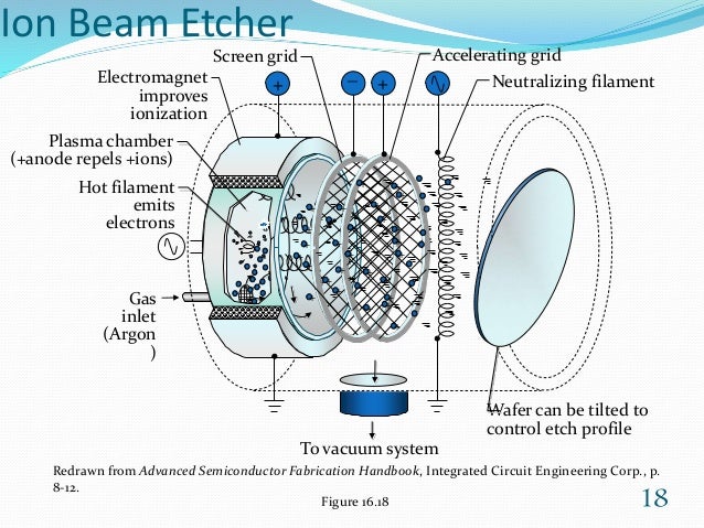
In essence an ion beam source is a plasma source having a set of grids that enable extraction of a stream of ions.
In this process the sample material is bombarded with high energy argon ion beams in a high vacuum chamber.
The number of electric short fails increases markedly at an ion beam angle greater than 35.
Reactive ion etching rie is an etching technology used in microfabrication.
The electric short fail trend of the perpendicular magnetic tunnel junctions p mtjs caused by the ion beam etching ibe process is studied at various ion beam angles and cell to cell space widths.
Rie is a type of dry etching which has different characteristics than wet etching.
The three main parts of the ion beam source are the discharge chamber the grids and the neutraliser.
Ion beam etching or milling is achieved by directing a beam of charged particles ions at a substrate with a suitably patterned mask in a high vacuum chamber.
Rie uses chemically reactive plasma to remove material deposited on wafers.
The plasma is generated under low pressure vacuum by an electromagnetic field.
Thereby argon ions are radiated onto the surface as an ion beam with about 1 to 3 kev.
Focused ion beam also known as fib is a technique used particularly in the semiconductor industry materials science and increasingly in the biological field for site specific analysis deposition and ablation of materials.
Ibm or etching is generally a surface finishing process in which the material removal takes place by sputtering of ions.
This can lead to increased etching rate or higher material selectivity of the etching process.
Oxford instruments plasma technology is a world leader in plasma process solutions with a long history of providing the latest technology innovations in plasma processing.
A fib setup is a scientific instrument that resembles a scanning electron microscope sem.
The wafer is held perpendicular or tilted into the ion beam the etch progress is absolute anisotropic.
Because of the energy of the ions they strike out material of the surface.
Plasma and ion beam etching deposition technology.
Ion production is done in the discharge chamber by subjecting a gas like argon to an rf field.
.jpg)